PCB Assembly
- PCBA Products
PCBA Products
- PCBA Capability
PCBA Capability
- PCBA Service
PCBA Service
- PCBA Factory Tour
PCBA Factory Tour
- PCB Component sourcing
PCB Component sourcing
“EXCEEDING” PCB Assembly offers a comprehensive printed circuit board assembly service that covers every aspect of the process, from initial part procurement to final shipping. Utilizing a blend of cutting-edge technology and skilled craftsmanship, we ensure precision and quality at every step. The service includes meticulous planning based on an approved Bill of Materials (BOM), precise solder paste application, automated and manual component placement, and a variety of soldering methods tailored to each project's unique requirements. Advanced inspection techniques, such as 3D Automated Optical Inspection (AOI) and X-Ray technology, are employed to guarantee the highest quality standards. The end result is a meticulously assembled PCB, cleaned and packaged with industry-standard materials, ready for immediate integration into your projects.
Our expertise extends to a range of specialized services:
•Custom Printed Circuit Board Design: Tailored to your specific needs, ensuring high performance and reliability.
•Precision PCB Assembly: Meticulous assembly processes to bring your designs to life with exceptional accuracy.
•Advanced X-Ray Inspection: Utilizing cutting-edge technology to ensure the highest quality and integrity of your PCBs.
Our Process:
1. PROCUREMENT AND PLANNING
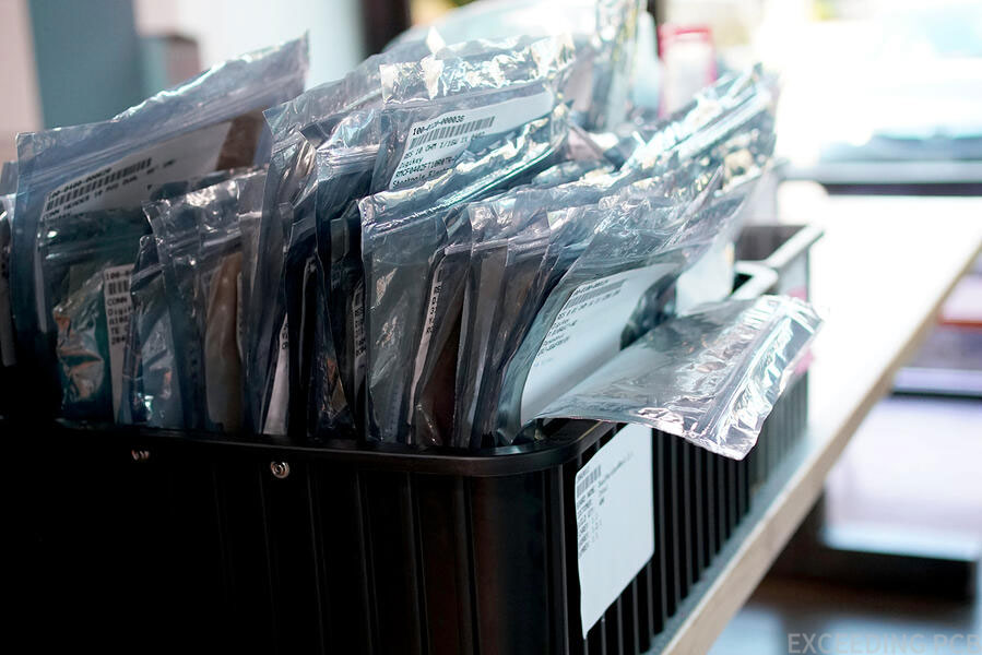
Starting a PCB project kicks off with acquiring the necessary parts. After the project's specifications are set, we source the components and create a Bill of Materials (BOM), detailing each component, its manufacturer, and delivery information. Once you approve the BOM, we order the parts. Your project officially starts when these parts arrive. Upon arrival, we categorize the parts by project, scan them into our system, and track them during the PCB assembly. This meticulous process guarantees precise component placement and allows us to pinpoint and resolve any issues efficiently.
2. SOLDER PASTE
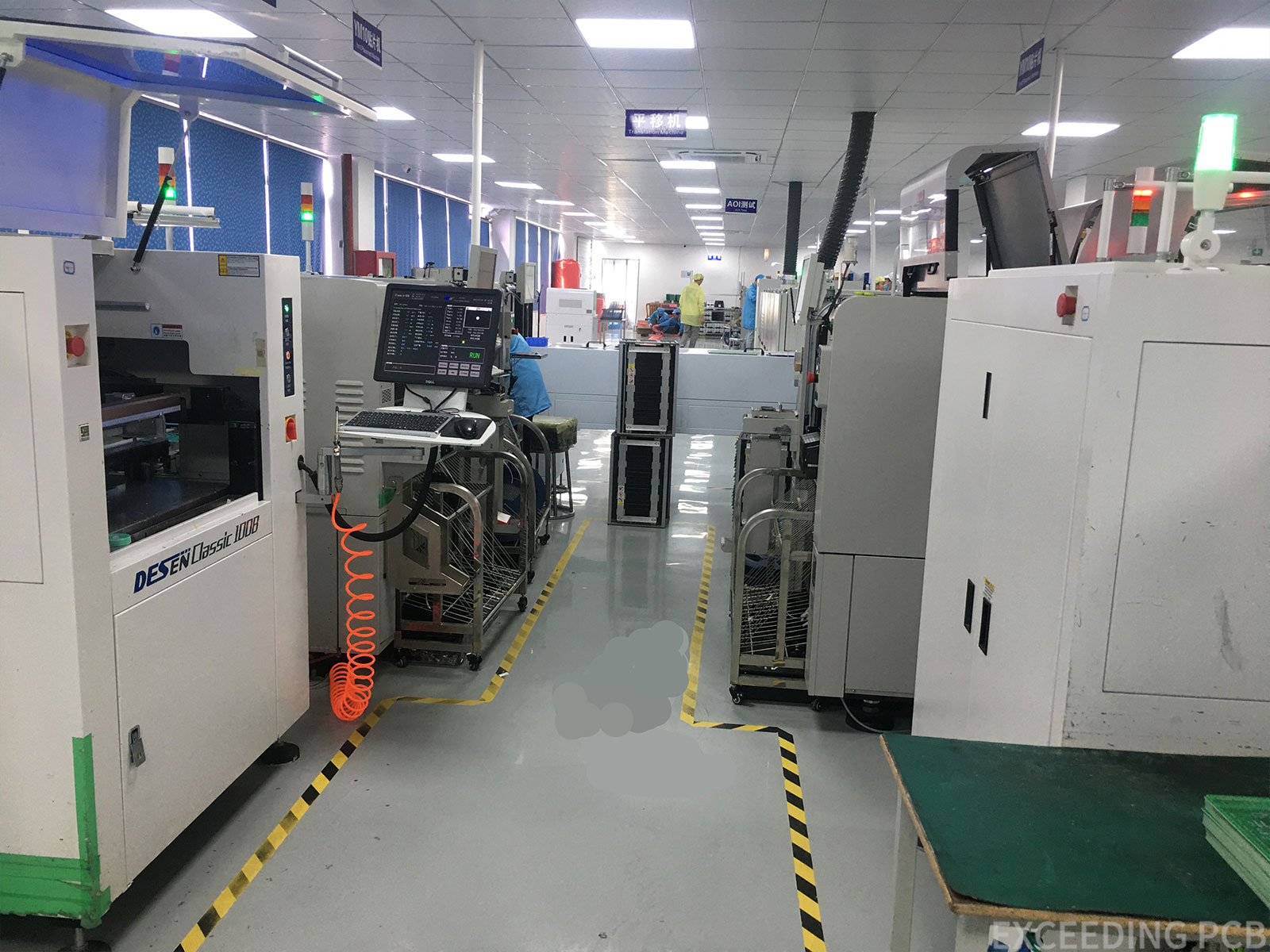
Before attaching components to a PCB, solder paste must be precisely applied to specific areas, primarily the component pads. This paste is a mixture of metal alloy powder and flux, a putty-like substance, and applying the right amount is critical to avoid misalignments or poor connections. There are two methods for this: using a solder screen or a jet printer. The solder screen, created during the board design process, has holes aligned with the board's solder-required areas. Paste is spread over the screen and then scraped through the holes to the board. In contrast, a jet printer, which is like a conventional printer, receives coordinates for where to apply paste and precisely deposits it in tiny dots on the component pads. While jet printers are more accurate and reduce solder waste, they are not as quick as the screen printing technique.
3. COMPONENT PLACEMENT
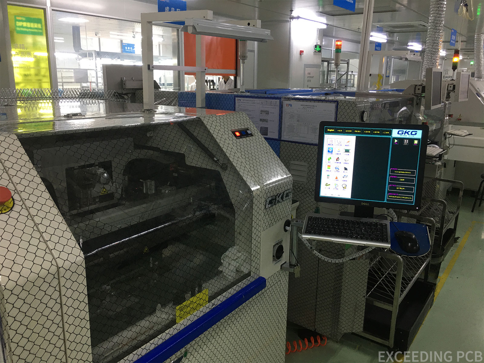
Following the solder paste application, boards now termed 'wet boards' are ready for component placement. While some larger or through-hole components are manually placed, most components are positioned onto the board using pick and place machines. These machines function as their name implies: they pick up each component and place it accurately on the board. Components are loaded into the machine in reels, and using specialized software, the precise location and orientation of each part are programmed. During operation, one or multiple heads of the machine pick up the components, align them as per the design specifications, and place them onto the wet solder. This holds the components temporarily in place until they are permanently affixed through the soldering process.
4. SOLDERING
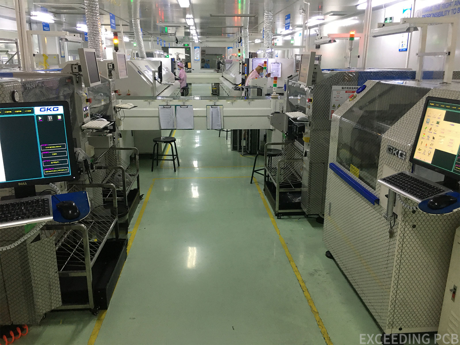
After a board is fully assembled with components, the next step is to melt the solder to permanently attach these parts to the board. This process varies based on the component's size, placement, and type, and can be done through hand soldering, reflow ovens, or selective soldering methods. In reflow ovens, boards are moved on conveyor belts through various heating and cooling zones. Technicians tailor the conveyor's speed and the temperature in each zone to create specific time-temperature profiles, ensuring the solder melts as needed for each specific project. Selective soldering, on the other hand, involves a nozzle guided by a set of coordinates to apply a targeted molten solder fountain to unsoldered components. This method is particularly useful for parts that need soldering after initial reflow oven processing, requiring precision to avoid damaging adjacent, already soldered parts. If selective soldering isn't suitable, our skilled technicians undertake hand soldering, using state-of-the-art Metcal soldering equipment, to ensure the highest quality in PCB assembly.
5. INSPECTION
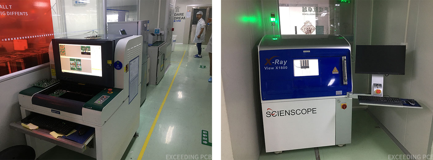
Inspections in PCB production are integral and occur at multiple stages, including key Automated Optical Inspection (AOI) checks on wet boards for solder paste. However, the bulk of inspections are conducted post-completion, as manual checking of surface mount boards with extensive components is impractical. Instead, 3D AOI and X-Ray technologies are utilized for thorough analysis. AOI uses intense light flashes to reveal imperfections and read part numbers, quickly assessing each component's presence, location, and orientation, and detecting issues like bent or lifted leads with its volumetric height measurement. X-Ray inspection, essential for uncovering internal defects and examining parts hidden by others, employs non-destructive techniques. While 2D X-Ray excels in individual board or component examination, particularly for void analysis, 3D X-Ray takes thousands of images to reconstruct detailed views of whole or parts of boards and components, ensuring even the smallest elements are meticulously inspected.
6. CLEANING, PACKING, AND SHIPPING
Once all required components are sourced, soldered onto the boards, and the boards have successfully passed all necessary inspections, they are nearly set for dispatch. The final step involves a gentle cleaning process to eliminate any residual solder paste, glue, or other substances acquired during assembly. After this, the boards are meticulously packaged using industry-standard, antistatic materials, ensuring their safe and secure delivery to the customer.

Address: Room 1107, Building 3, Country Garden Wisdom Apartment, Xingyi Road, Fuyong Street, Bao'an District, Shenzhen,China. Tel: (+86) 755-2733 1193
Email: sales@exceedingelec.com

Online Shop


